Design & Manufacturing
DenseLight provides one-stop design and manufacturing solutions, from photonics design and simulation, epitaxial growth, wafer fabrication, chip production, in-line optical coating, sub-mounting, photonic measurements, product tests and screening.
DenseLight is operationally ready for responsive prototyping and quality production. The 50,000 sq. ft. purpose-built facility houses its headquarters, R&D, product design and manufacturing operations under one roof. Its 15,000 sq. ft. clean room is fully equipped for enabling vertically integrated volume manufacturing, from wafer fabrication to test and packaging.
We have an experienced team with deep know-how in InP semiconductors wafer processing. Together with operationally ready manufacturing and photonics design centre, various ODM and Design-In programs can be supported for both discrete and integrated optical components. These advanced modules include: Hybrid/monolithic photonics integrated circuits. Find out more about our Photonic integration technology >>
Customized photonics devices and arrays
DenseLight prototyping allows an outsourced photonic supply chain where it is feasible for firms to segregate design, manufacture and distribution activities reducing the need for heavy capital investments.
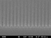
InP array waveguide grating structure fabricated |
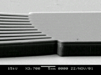
0.12um features defined by |